Mirley - Electronics & Programming
projects, programs... all about electronics


Before you start work, make sure you have the rubber gloves and other protective measures. Do not drink etchant (as well as other chemicals) or place it near food, etc. After work, always wash your hands.
What's Needed:
- Chalky Paper (for thesis printing, available in the office shops)
- Laser printer or access to photocopier
- Copper Clad PCB cutted to the right size
- Iron
- Digestion Liquid (water solution of Sodium Persulphate, B327)
- Drill with 1 mm, 1.2 mm, 3 mm drill bits
- Solvent solution of colophony and brush
Realization:
1. PCB Design
Prepare PCB using dedicated software (without mirror image)2. Printing the PCB Drawing
We print PCB drawing on chalk paper using a laser printer (high resolution, dark). If the laser printer is not available we can print PCB on any printer and than make photocopy on chalk paper. Make sure that PCB is printed in scale 100%, without any options like: "fit to page". In all designs presented on my website, the extra 3 cm line was placed on PCB. It will be helpful when we not sure that the print scale is good. When we already have the print, which looking like this in the picture below, we can follow to the next step.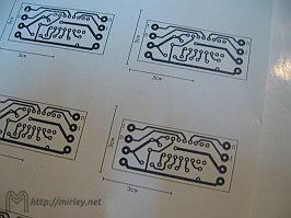
3. Preparing Copper Clad PCB and Prints
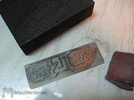
We cut out PCB picture, which was printed in previous step and we prepare a piece of one-sided copper clad laminate. Now we cut out the laminate to the right size, according to the PCB dimensions or a little bigger. For this, the hacksaw, the sheet metal cutters or wallpaper knife (it depends on our possibilities and skills) can be used. We can polish and round off the edges of the laminate. It will improve the visual appearance. After use the sandpaper or the abrasive sponge we should clean the area of laminate and get rid of contamination and copper oxide. After brushing we need to be careful and don't touch polished and cleaned area.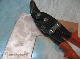
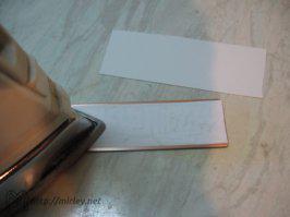
4. Ironing
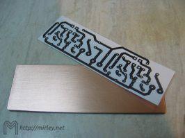
Prepare an iron and something (eg. wooden board), which will be needed as a support during ironing the PCB. If is possibility to use the old iron, it will be good choice, and not that which will later be used to ironing shirt :). Put the print on the laminate and slightly iron the print to the copper. When the print is glued to the copper side of the laminate, we put another piece of any clean paper (to keep the iron clean) and the iron on the top. Iron should cover entire board. It should be hold the iron in this position some time, dependent on the temperature and iron power. If the chalky paper, placed on the top, will get slightly brown (from time to time we need to put off the iron and check) it should already be long enough. When we are ironing the PCB, is very important to not move print relative to the laminate. In other way we will see the fuzzy tracks on the PCB, especially for small laminates.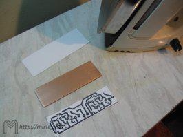
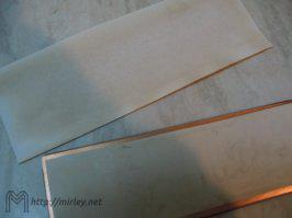
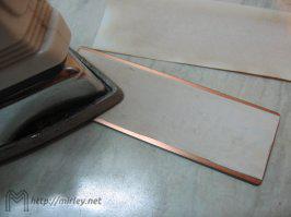
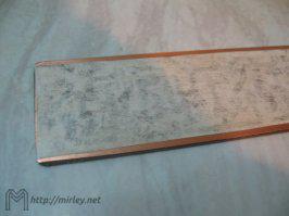
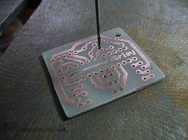
5. Removing of the Paper
After thermotransfer, we should wait several minutes until the laminate cooled off. In the meantime a container with warm water and a drop of dishwasher liquid should be prepared. After cooling the laminate put it into the container with soapy water and wait a moment until the chalky paper become soaked. In the next step we remove gently the paper, but toner should stay glued on copper side of the laminate. Take your time in this step because the paper should be completely removed from the laminate. This requires a bit of work but it is necessary for good final result. Remains of paper between tracks may hinder digestion and as a result may even lead to a short circuit on the board. After drying broken tracks can by fixed by PCB marker.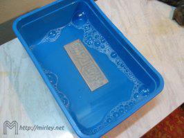

6. Preparing of Sodium Persulfate
Prior to digestion we prepare the container (eg. 1 liter jar) glass or plastic, which will serve as a simple digestion container. Typical package of etchant (B327) needs around 0.5 liters of warm water (50 degrees). The whole should be stirred until complete dissolution. After cooling to a temperature of about 40 degrees etchant is ready for operation.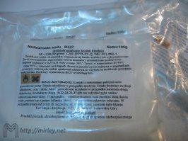

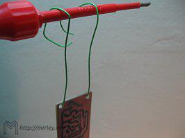
7. Preparing PCB for Etching
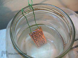
Etching PCB can be removed from jar only by instruments made of plastic or wood. Metal reacts with the Sodium Persulfate. I personally recommend another way to put the PCB into etchant. Usually the PCB has mounting holes, which should be drilled before etching. If mounting holes are not foreseen in PCB design, a two additional holes in place where are no tracks will be necessary. To place board in vertical position in jar an isolated wire can be used. Using such a wire provides easy way to insert and remove the PCB from the etchant without dirtying your hands.
8. Etching
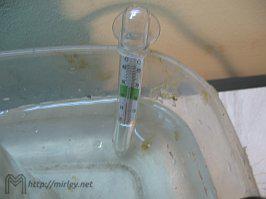
Etching process is optimized in temperature of 40 degrees, so is good to keep the digestion solution in this temperature all the time during the etching process. The glass jar we can simply place inside bigger container, which can be filled by hot water, which keep the etchant warm. The temperature of the water can be kept by any heater (eg. aquarium heater). It's good to use thermometer during warming process to avoid overheating, which can demote the quality of the PCB tracks. Temperature of the etching process (40 degrees) has important meaning and allows to quicker etching. The PCB orientation (vertical, horizontal) is also important aspect, because the whole process is faster when the board is hung in a vertical position (see in section 7). This method allows to better controlling the whole etching process.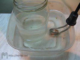

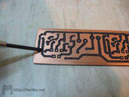
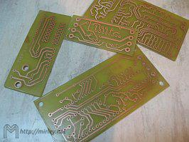
9. After PCB Etching
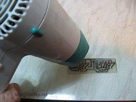
If between the PCB tracks the copper is no longer present, we remove the board from the etchant. After that the PCB should be precisely washed up by tap water and allow to dry. For improve safety a rubber gloves can be used. In next step the toner should be removed, by using sandpaper or an abrasive sponge. Our eyes should see the beautifully etched tracks. We drill holes 1mm for standard components and 1.2mm for bigger ones. Now we should grind the PCB again to get rid of burrs on the copper, produced during drilling. In addition, using an abrasive sponge we can grind the other side of the laminate. At the end we cover copper tracks (with a small brush) by colophony dissolved in alcohol or solvent. After that we leave it to dry for the whole day or if we don't have much time, we can speed up this process by using a hair dryer.
10. Storage of Sodium Persulfate
When the etching process is finished, the etchant should be stored in safe place, away form children. The jar with etchant shouldn't be curled hard, because the gas created inside the jar may destroy it. The good solution is to create small hole in jars lid.Questions and Comments:
comments powered by Disqus
July 19, 2018
Power supply was presented ...
More …
June 20, 2018
Triac Module was presented...
More …
More news …
Power supply was presented ...
More …
June 20, 2018
Triac Module was presented...
More …
More news …

Recommended Sites